Common Base
Configuration
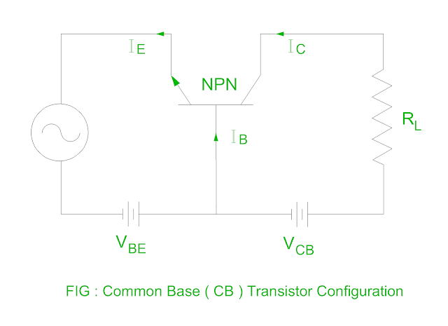
- As the base terminal is common to both input and output of the transistor, it is called as Common Base Configuration.
- The input voltage VBE is applied between base and emitter terminal whereas the output is taken from collector and base terminals.
- The common base configuration for NPN transistor is shown in the Figure.
Current
Amplification Factor
- It is defined as the ratio of the output current ( collector current ) and input current ( emitter current ).
- It is ratio of the change in collector current to the change in emitter current at constant collector – base voltage ( VCB ).
α = dIC / dIE
- As the emitter current is always greater than collector current, the current amplification always less than unity.
- The current amplification factor can be increased by decreasing base current.
- The base current is increased by making base thin and lightly doped.
- The range of current amplification factor lies from 0.9 to 0.99.
Expression of
Collector Current
- The collector to base junction is reverse biased, therefore the collector current flows due to minority charge carriers.
- This current is called as leakage current.
Total collector
current
IC = αIE
+ ILEAKAGE
- As the emiiter is open circuit, small leakage current flows in the collector circuit. This leakage current is called as ICBO.
ICBO
= Collector to base current with emitter open
IC =
αIE + ICBO ……… ( 1 )
As IE
= IC + IB
IC =
α ( IC + IB ) + ICBO
IC =
αIC + αIB + ICBO
IC – αIC = αIB + ICBO
IC (
1 – α ) = αIB + ICBO
IC =
αIB / ( 1 – α ) + ICBO / ( 1 – α )………….. ( 2 )
Characteristic
of CB Transistor Configuration
Input
Characteristic
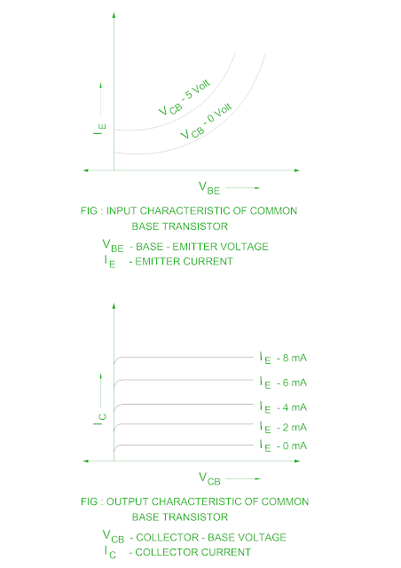
- It is relation between emitter current and emitter – base voltage at constant collector – base voltage.
- The emitter current is taken along Y – axis and emitter – base voltage is taken along X – axis.
Key Points
- As there is small increase in input emitter – base voltage, the emitter current increases rapidly.
- It means that input resistance is very small.
- The input current does not depend upon output collector – base voltage.
Input resistance
= dVBE / dIE
Output
Characteristic
- It is relation between collector current and collector – base voltage at constant input current ( Emitter current ).
- The collector current is taken along Y – axis and collector – base voltage is taken along X – axis.
Key Points
- As the collector – base voltage increases, the collector current becomes almost constant.
- It means that the output or collector current does not depend upon collector – base voltage but it depends upon input current or emitter current.
- As the emitter current increases, the collector current also increases.
- As the change in collector to base voltage is very large, there is no change in the collector current it means that output resistance is very high.
Output resistance
= dVCB / dIC at constant IE
How the current amplification
factor can be increased?
- The current amplification factor can be increased by decreasing base current or by making base very thin.
Describe the
range of current amplification factor for common base configuration.
- 0.9 to 0.99
The input
resistance of CB configuration is very high – Give reason.
- The input emitter current increase very rapidly in spite of small change in input voltage, it indicates that the input resistance of CB configuration is very small.
The output
resistance of CB configuration is very low – Give reason.
- The output current of the CB configuration remains constant in spite of large change in output current it indicates that the output resistance of CB configuration is very large.
What do you mean
by ICBO?
- It is leakage current, the ICBO indicates that the output or collector current flows when emitter to base junction ( input ) is open circuited.
You may also like :


No comments:
Post a Comment