- The power circuit diagram of the single phase parallel inverter is shown in the figure A.
- The commutating capacitor C is connected across supply source therefore it is called as PARALLEL INVERTER.
- The turns ratio of half primary winding and secondary winding is kept unity.
- The SCR T1 and SCR T2 are main SCRs from which load current passes through it.
Mode 1
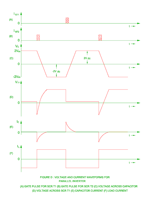
- The load current flows through path +Vdc – L – c – a – SCR T1 – Vdc when the SCR T1 is turned on.
- This will generate flux and resulting emf in the transformer primary winding ac and bc.
- The charging of capacitor is done up to 2Vdc voltage due to these induced emf.
- The polarity of capacitor C is done in the figure B.
- The maximum voltage withstand capability of the SCR T2 is 2Vdc.
- The induced emf in the transformer secondary is 2Vdc as there is unity turns ratio between half primary and secondary winding.
- This will result flow of current through load.
|
Read More Minimum clearance
between transmission line conductor and ground Minimum clearance
between transmission line when they cross to each other Function of Earthing Conductor |
Mode 2
- When the SCR T2 is turned on, the SCR T1 is turned off due to capacitor reverse voltage 2Vdc applied across it.
- As the SCR T2 is turned on, the load current flows through path +Vdc – L – c – b – SCR T2 – Vdc and discharging of capacitor is done through SCR T2.
- The charging of capacitor again done with – 2Vdc voltage.
- The current flows during this interval are in reverse direction as that of when SCR T1 is turned on.
- The SCR T1 again turned on when it receives gate pulse and SCR T2 is in off condition during this interval.
- The waveform of the output voltage become rectangular due to alternately switching of SCR T1 and SCR T2.
Parallel inverter with feedback diodes
- When load is inductive, the load current becomes out of phase with load voltage and direction of load current reverses with respect to load voltage.
- The stored energy during this interval feeds back through diodes D1 and D2.
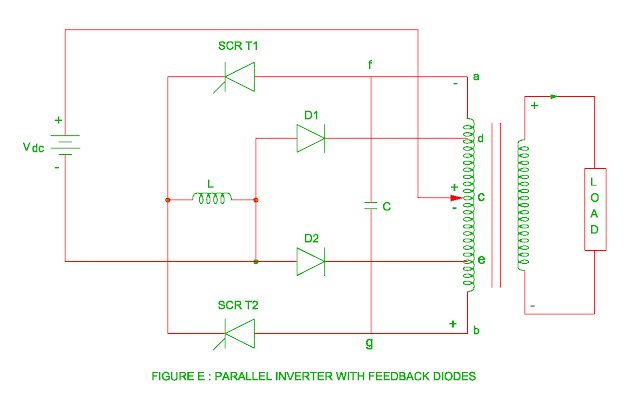
- The circuit diagram of parallel inverter with feedback diodes is shown in the figure C.
- When SCR T1 is turned on, flow of current through path + Vdc – c – a – SCR T1 – L – Vdc (-).
- The flux generated in the transformer primary winding ac and bc due to this current.
- This will result in 2Vdc voltage induced in the transformer primary winding.
- The charging of capacitor polarity is shown in the figure D.
- When SCR T2 is switched on, the SCR T1 is turned off due to reverse voltage of capacitor and capacitor discharges through path C – g – SCR T2 – L – D1 – d – a – f – C.
- The stored energy of capacitor transfers to load via transformer upper side primary winding.
- When SCR T2 is turned on, the current flows through path + Vdc – c – b – SCR T2 – L – Vdc(-) and capacitor again charges with voltage – 2Vdc.
- The capacitor again discharges through path C – f – SCR T1 – L – D2 – e – b – g – C when SCR T1 is again turned on.
- This will result in stored energy of capacitor transfer to load via transformer lower side primary winding.
Advantages
- Simple forced commutation circuit.
- Sinusoidal waveform at output is possible by using suitable filter circuit.
Disadvantages
- The parallel inverter is useful only when load is fixed. (The output waveform changes due to change in load )
- The inverter does not useful for higher power for fixed value of inductor L and capacitor C.
- The design of inverter is done for fixed voltage.
You may also like :
Semiconductor Memories Interview Question Answer - 1
Semiconductor Memories Interview Question Answer - 2
Magnetic Hysteresis Interview Question Answer - 1
Magnetic Hysteresis Interview Question Answer - 2
Design of Magnetic Circuit Interview Question Answer - 1
Design of Magnetic Circuit Interview Question Answer - 2


